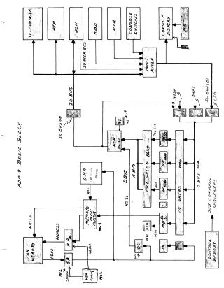
PDP-9 Basic Block
Order Number: XX-AD55D-9E
This document presents a detailed technical overview of the PDP-9 computer system, encompassing its fundamental architecture, operational timing, software instruction logic, and specific hardware component designs.
The document begins with a basic block diagram of the PDP-9, illustrating its memory, various buses (IO, A, B, O), and connected input/output devices such as the Teletype, PTP, KBD, PTR, Console Switches, and Console Display. It provides timing diagrams for core system operations, including main memory access, execute cycles, program interrupts (PI Timing), and real-time clock (RTC) functions.
Specific instruction logic diagrams detail the internal workings of various PDP-9 instructions, including LAC, AND, SAD, IAO (DAC, CAL, JMS, DZM), ADD, XCT, XOR, JMP, ISZ, and TAD, showing how they interact with registers and buses. A memory reference instruction demonstration program provides mnemonic code and its encoded representation.
Furthermore, the document includes detailed schematics and functional descriptions for critical hardware components. These include the Control Memory Driver G210, the S202 Flip-Flop, the B213 Flip-Flop, and the B-131 Adder. The adder's summing and carry networks are explained in depth, complete with transistor conduction states and input/output tables. The document also provides extensive tables depicting bit sequences and operational states during tape handling, specifically for "Tape Traveling in Forward Direction" and "FWD End Zones."
Site structure and layout ©2025 Majenko Technologies