Console Board
Order Number: XX-CCD3C-5D
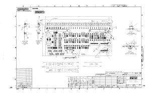
This document is a multi-sheet schematic diagram detailing the design and functionality of a Console Board. It illustrates the board's electrical connections, logic, and interfaces across different functional blocks identified as KNLA, KNLB, KNLC, and KNLD.
Sheet 1 provides the overall layout, power supply connections (+5VA, +5VB, +5VC), ground signals (GNDA, GNDB, GNDC), and a table for IC pin locations. It also includes copyright and ownership information for the drawing and specifications.
Sheet 2 (KNLA) focuses on the KNL/PDR (Processor Data Register) Interface, showing the logic for various "KNLA DISP" (display) signals and panel lock inputs, implemented with 7404 logic gates and resistors.
Sheet 3 (KNLB) outlines the KNL/SCC (System Console Controller) Interface, detailing the logic for "KNLB DISP ADRS" (address display) signals and several "KNLB IND" (indicator) signals, including PAUSE, ADDRESS ERROR, MASTER, RUN, and PARITY ERROR.
Sheet 4 (KNLC) presents the KNL SCC Interface, specifically covering "KNLC SWR" (switch register) inputs from switches S1 through S22, and the logic for various "Console Switches." These include control, single bus cycle, load address, start, examine, deposit, and halt functions.
Sheet 5 (KNLD) integrates detailed logic for display registers, address/bus registers, data paths, and the handling of 16-bit, 18-bit, and 22-bit memory mapping. It also includes tables defining code select lines for user, kernel, program, and console functions, as well as mappings for bus register, data path, display register, and address functions.
Overall, the document serves as a comprehensive technical blueprint, detailing the Console Board's internal logic, interconnections, and interfaces within a larger system.
Site structure and layout ©2025 Majenko Technologies