DEC-10-HMBB-D KA10 Maint Vol2 Set2
Order Number: XX-7C735-18
This document is a multi-page alphabetical index and signal glossary for a KA10 processor, likely a component of a larger computer system.
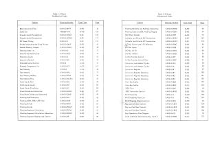
The first two pages list subjects, drawing numbers, type codes, and page references, forming an alphabetical index for various components, functions, and control mechanisms within the KA10 processor (e.g., "Byte Instruction Flow," "Fast Memory," "Floating Divide," "I/O Bus Control").
Pages 3-14 provide a "KA10 Signal Glossary," detailing numerous signal names, their source drawings, and concise descriptions of their function within the KA10 system (e.g., "ADO-35: Adder. Performs arithmetic and logical operations," "AR DCK: Divide check flag. Set when fractional dividend not smaller than divisor").
Pages 15-19 present a "Master Drawing List," which is another index organized by drawing number, revision letter, number of sheets, and title (e.g., "KA10 ASSEMBLY," "ADDER CONTROL FLIP-FLOPS," "MODULE UTILIZATION PANELS").
Pages 20-23 contain a detailed drawing index that visually categorizes various mechanical and electrical components and their respective part numbers and descriptions.
Pages 24-25 include an "Engineering Specification" for "Removing and Reinstalling the KE10 Option: Byte and Floating Point," outlining a step-by-step procedure for hardware modification, including module removal/installation and jumper connections, followed by diagnostic testing.
Pages 26-28 provide another "Engineering Specification" for "Removal and Re-Installation of KM-10 'Fast Registers'," detailing similar hardware modification and testing procedures.
Pages 29-30 describe the "Removing and Re-Installing the KT10 Option: 'Time Sharing Option'," with instructions for module handling and diagnostic checks.
The remainder of the document (pages 31-193) consists of numerous detailed circuit diagrams and wiring schematics (e.g., "Basic Instruction Flow," "Floating Divide," "Memory Control," "AR Register," "Parity Network," "I/O Bus," "Shift Count Register," "Program Counter Control," "Module Utilization Panels," "DC/AC Power Wiring," "TTY Socket Wiring," and "Twisted Pair Lists"). These diagrams illustrate the intricate interconnections and logic of the KA10 processor's various sub-systems, including detailed component names, pin references, and signal flows.
Site structure and layout ©2025 Majenko Technologies