W107
Order Number: XX-C1E50-1D
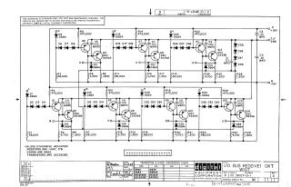
This document is an electrical schematic titled "I/O BUS RECEIVER CKT. W107," identified as W107-0-1, Revision A. Created by Digital Equipment Corporation in March 1967, it explicitly states that the schematic is for test and maintenance purposes only and the circuits are proprietary and copyrighted.
The schematic illustrates a complex circuit design, primarily consisting of multiple, largely identical input receiver stages (labeled L, D, F, J, T, N, R, S, U). Each stage typically includes:
- Input diodes (e.g., D1, D5, D15).
- A series of three diodes (e.g., D2-D4, D6-D8).
- A pair of transistors (e.g., Q1/Q2, Q3/Q4) with associated capacitors (e.g., C4, C5) and numerous resistors.
- An output diode (e.g., D9, D11, D19).
The circuit is powered by +10V, -15V, and ground (GND) lines. General component specifications indicate that resistors are 1/4W, 5% tolerance; diodes are D662; and transistors are DEC3639C, unless otherwise noted. A "Transistor & Diode Conversion Chart" provides cross-references between DEC part numbers (D662, D664, DEC3639B, DEC3639C) and their EIA equivalents (IN645, IN3606, 2N3639).
Site structure and layout ©2025 Majenko Technologies