M7100
Order Number: XX-39EB6-3E
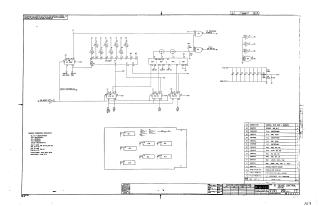
This document is a proprietary schematic diagram from Digital Equipment Corporation for the "IO DEVICE CONTROL M7100" module, dated 1970 and intended for test and maintenance purposes.
The schematic illustrates a digital circuit designed to manage Input/Output (IO) operations. It features several key functional blocks:
- Input Conditioning: Buffers and processes various input signals, including "PI SYNC" (Program Interrupt Synchronization), "IOB PI REQ SYNC", "DEV PI REQ", and "RESET BUFFERED (L)".
- Decoding: A "DECODER E4" likely interprets address or control inputs to generate internal selection signals.
- Comparison: A "COMPARATOR E2" is present, possibly for address matching or status comparison related to IOB00, IOB01, and IOB02.
- Peripheral Interface: Multiple "Peripheral Interface Adapters" (PIA 33, 34, 35) are central to the module, facilitating communication and control with I/O devices.
- Response Generation: Logic is included to generate a "PI RESPONSE ENABLE" signal.
- Power and Filtering: Standard power supply connections (+5V, +3V, GND) are shown along with various capacitors and resistors for filtering and voltage regulation.
The module primarily uses integrated circuits from the DEC1074 series (H04, H11, H74) and DEC82xx series (8251, 8242), along with discrete resistors and capacitors, as detailed in the accompanying parts list.
Site structure and layout ©2025 Majenko Technologies