M707
Order Number: XX-F1F7F-8B
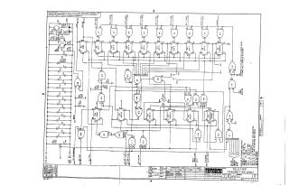
This document is a schematic diagram for a Digital Equipment Corporation (DEC) Teletype Transmitter M707, copyrighted 1967.
The circuit primarily functions as a parallel-to-serial converter for Teletype data transmission. Key components and features include:
- 8-Bit Data Register: A series of D-type flip-flops (E7, E15, E11, E5, E8, E6) labeled "BIT 1" through "BIT 8" are used to store the parallel data character to be transmitted. These bits are loaded from "DEVICE SELECTOR INPUTS FROM BMB."
- Stop Bit Generation: Flip-flops (E17, E14) are dedicated to generating the necessary stop bits (1, 1.5, or 2) for Teletype communication protocols.
- Baud Rate Generation: A "FREQUENCY DIVIDE" flip-flop (E14) and associated logic derive the appropriate transmission baud rate from a "2 X BAUD CLOCK INPUT."
Control and Status Logic:
- "ENABLE" flip-flop (E4) controls the transmission sequence.
- "FLAG" and "ACTIVE" flip-flops (E16) provide status indications.
- Inputs like "I/O SKP," "I/O SXP STROBE," "P.I. REQ.," "CLEAR FLAG 2," "I/O CLEAR," and "WAIT" are used for loading data, initiating transmission, and managing the process.
Input/Output Buffering: Transistors (Q2, Q3) and associated resistors (R7-R9, R12) along with capacitors (C20-C22) likely condition the "LINE" and "ACTIVE" input signals. Logic gates (E1, E4) buffer the output, labeled "ASD LOAD BUFFER."
- Power Supply: Operates with +3V and +5V rails, with various filtering capacitors (C2-C18).
- Component Technology: Utilizes early integrated circuits (indicated by DEC7474N, DEC7430N, DEC7400N series logic) and discrete transistors (DEC3009B, DEC6534B).
In essence, the M707 takes parallel data, converts it into a time-sequential serial stream, and adds the necessary start/stop bits and timing for communication over a Teletype line.
Site structure and layout ©2025 Majenko Technologies