M7050
Order Number: XX-8C471-84
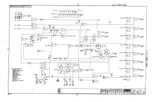
This document is a detailed schematic diagram for a "READER CONTROL" unit designed by Digital Equipment Corporation in 1971.
The circuit primarily functions to read data from a physical reader (likely a paper tape or punch card reader) and interface it with a digital system's I/O bus, while also managing reader control and status.
Key functionalities and components include:
- Input Conditioning: Various input lines, including "MB 3(0)" through "MB 8(1)" and "IOP 1(1), 2(1), 4(1)", are processed through logic gates (DEC7400, DEC7401, DEC7430) and inverters (DEC7404, DEC7440) for initial signal decoding and conditioning.
- Reader Data Acquisition: The core data input comes from multiple "RD HOLE" lines (RD HOLE 1 through RD HOLE 8). Each "RD HOLE" input feeds into D-type flip-flops (DEC7475, DEC7474) which latch the state of these physical holes. The latched data is then buffered and output onto the system's I/O bus as "I/O BUSS IN4" through "I/O BUSS IN11", indicating an 8-bit parallel data path. A "FEED HOLE" input also exists for synchronization.
- Control and Status:
- "ON/OFF LINE" (BUI): A control line for enabling or disabling the reader.
- "OUT OF TAPE" (BL2): A critical status output indicating when the reader media has run out.
- "RUN" (E5): A flip-flop indicating the active operating state of the reader.
- "FLAG" (E5): A general status flag.
- "POWER" (BR2): An output likely indicating the reader's power status.
- I/O Bus Control: Signals like "I/O BUSS IN SKIP" (AK2) and "I/O BUSS IN INT" (AL2) provide control directives to the I/O bus for operations like skipping data or triggering interrupts.
- Operational States: Logic involving "CLK-BBI", "STOP-BN2", and "COMPLETE-BNI" manages the start, stop, and completion of reader operations.
- Initialization & Shift: Inputs like "INITIALIZE BPI" and "SHIFT BJI" provide reset and data shifting commands.
- Timing and Buffering: The schematic includes a "CLOCK I" input, monostable multivibrators (DEC9601 - implied by "E3 7ms"), various gates, and discrete components (resistors, capacitors, diodes, and MPS6531 transistors) for signal buffering, timing, and power supply decoupling (+5V(A) and +5V(B)).
In essence, the "READER CONTROL" circuit is an interface logic board designed to manage the electromechanical operation of a data reader, translate its physical hole detections into digital bus signals, and report its operational status to a larger computer system.
Site structure and layout ©2025 Majenko Technologies