M703
Order Number: XX-23B24-6D
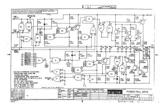
This document is a schematic for a "POWER FAIL M703" module, designed by Digital Equipment Corporation in 1967.
Its primary purpose is to detect and signal a power failure condition within a larger electronic system. The circuit takes various inputs, including:
- "PWR LOW (1)" and "PWR LOW (0)" signals, likely indicating different power supply states.
- An "INITIALIZE S2" signal.
- A "STOP O.K. P2" signal.
- A "SHUT DOWN" input (U2) with multiple module-specific lines (MB3-MB8, IOP2) that feed into a "L2 PWR SKIP" output, suggesting power sequencing or bypass control.
The circuit utilizes a combination of proprietary Digital Equipment Corporation integrated circuits (designated E1 through E7, including types like DEC7400N, DEC7460N, and DEC7430N), discrete transistors (DEC6534B, DEC3009B), resistors, capacitors (including large electrolytic ones like C13 and C14 for timing/filtering), and diodes. These components form complex logic gates and transistor switching stages to process the input signals, detect power anomalies, and generate the appropriate "power fail" output signal.
The schematic is provided for test and maintenance purposes, and the circuits are noted as proprietary.
Site structure and layout ©2025 Majenko Technologies