M111
Order Number: XX-8EBAF-CC
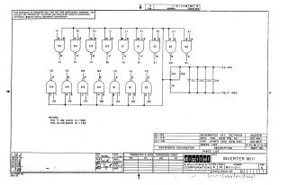
This document is a proprietary schematic diagram for an "INVERTER MIII" circuit, copyrighted by Digital Equipment Corporation (DEC) in 1968. It is furnished for test and maintenance purposes only.
The circuit design primarily features:
- Integrated Circuits (ICs): Specifically "DEC7400N" type (suggesting 7400-series TTL logic gates), including various logic gate types (E1, E2, E3, E4).
- Resistors: Three 750 Ohm, 1/4W, 5% carbon composition resistors (R1, R2, R3).
- Capacitors: Four 0.01µF, 100V disc capacitors (C1, C2, C3, C4) used for power conditioning.
Power connections for the ICs are noted: Pin 7 for Ground (GND) and Pin 14 for +5V, indicating a standard TTL operating voltage. The diagram shows the interconnection of numerous logic gates, powered by a +5V supply, with dedicated points for power (A2 +5V) and ground (C2, TI GND).
Site structure and layout ©2025 Majenko Technologies