M100
Order Number: XX-86FC0-1F
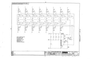
This document is a schematic diagram for the "BUS DATA INTERFACE M100," copyrighted by Digital Equipment Corporation in 1969. It is explicitly noted as being for test and maintenance purposes only, containing proprietary circuit information.
The diagram illustrates the detailed electrical design of the interface, featuring a complex arrangement of:
- Logic Gates: Primarily DEC 7400N series integrated circuits (likely NAND gates), organized into several stages (E1, E2, E3, E4) with numerous interconnections.
- Transistors: Multiple transistors (Q1-Q17, identified as DEC3009B and DEC6534B types, with EIA equivalents provided) used for input buffering, output driving, and power regulation.
- Resistors, Capacitors, and Diodes: A wide array of these passive and active components, with specified values and types (e.g., D662 diodes, 0.01 MFD capacitors).
- Power Supplies: The circuit operates with +5V, -15V, and GND connections, and includes a section that generates a +3V supply from these inputs.
Accompanying notes provide general component specifications, such as standard IC power pin assignments (+5V on Pin 14, GND on Pin 7 for each IC), default resistor wattage and tolerance (1/4W 5%), and a "Transistor & Diode Conversion Chart" mapping DEC part numbers to their standard EIA equivalents.
Site structure and layout ©2025 Majenko Technologies