G103
Order Number: XX-7ABC3-63
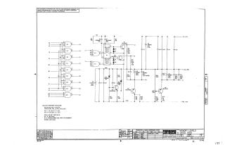
This document is an electrical schematic titled "MEMORY LEVELS & GATES G103" from Digital Equipment Corporation, copyrighted in 1969, and intended for test and maintenance of proprietary circuits.
The schematic illustrates a circuit that combines logic gating with transformer-coupled drivers and transistor switching stages, likely for controlling or interfacing with memory components.
Key features include:
- Logic Gates: A significant portion of the circuit utilizes multiple integrated circuits (E2, E4, E5 are DEC74H10; E3 is DEC7440), configured as logic gates (e.g., NAND gates). These gates process various input signals (P2, V1, J2, K1, F2, M2, M1, N1, U1, P1, R1, U2, V2, S1) to produce logical outputs.
- Transformer and Transistor Drivers: A transformer (E1, DEC Part # 1609996-0) is central to a section that includes transistors (Q1, Q2 - DEC2007) and associated diodes (D2-D5) and resistors (R3, R4). This part likely generates specific signal levels or drive currents for memory operations.
- Power & Output Stages: The circuit incorporates several transistors (Q3 - DEC3009A, Q4, Q5 - DEC3762) along with numerous capacitors and diodes (D1, D6) for power conditioning and signal processing. It operates using +5V and -15V power rails, with a common ground.
- Component Specifications: General specifications for resistors (1/4W, 5%) and capacitors (.01 MFD, 100V, 20%) are provided, with exceptions noted on the schematic. Specific power connections for ICs (Pin 7 = GND, Pin 14 = +5V) are indicated.
- Conversion Chart: A "Transistor & Diode Conversion Chart" is included, mapping some DEC part numbers (e.g., D664, DEC3009A) to their EIA equivalents (e.g., IN3606, 2N3009A).
Site structure and layout ©2025 Majenko Technologies