Diode Gate B117
Order Number: B-CS-B117-0-1
This document is a proprietary electrical schematic, copyrighted in 1964 by Digital Equipment Corporation (DEC), and is intended solely for test and maintenance purposes.
Key details from the schematic:
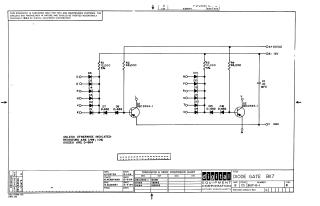
- Title: DIODE GATE BI17 (Drawing No. BI17-0-1, Rev. B).
Circuit Description: It depicts two identical multi-input diode-transistor logic (DTL) gates.
- Each gate has multiple inputs (D through K for the first, N through U for the second) that feed through diodes (D1-D6, D9-D14) to a common point.
- This common point then connects via two additional diodes (D7, D8, and D15, D16) to the base of a transistor (Q1, Q2, type DEC 2894-1).
- The circuit is powered by +10V(A) and -15V supplies, with an output taken from the transistor's emitter (L, V, M) to ground (GND). A 0.01 MFD capacitor (C1) is present between -15V and GND.
Component Specifications:
- Resistors (R1-R4) are generally 1/4W and 10% tolerance (unless otherwise indicated). Specific values are 12,000 ohms (R1, R3) and 68,000 ohms (R2, R4).
- Diodes (D1-D16) are primarily D-664 or D-662 types.
Conversion Chart: A "Transistor & Diode Conversion Chart" provides EIA equivalents for DEC parts:
- Transistor DEC 2894-1 has no EIA equivalent listed.
- Diode D662 is equivalent to 1N645.
- Diode D664 is equivalent to 1N3606.
Personnel & Date: The drawing was prepared by H. Porter (DRN) and checked by N. Perryman (CHK'D) with engineering by B. Scudney (ENG) around May 1964.
Site structure and layout ©2025 Majenko Technologies