Diode Gate B115
Order Number: B-CS-B115-0-1
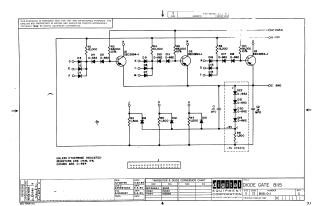
This document is an electronic schematic diagram titled "DIODE GATE BII5" from Digital Equipment Corporation, copyrighted in 1964. It is stated to be for test and maintenance purposes, describing proprietary circuitry.
The schematic illustrates a multi-input logic gate circuit primarily constructed using three NPN transistors (Q1, Q2, Q3, type DEC2894-1) and numerous diodes (predominantly D-662, which corresponds to IN645, with a general note that unspecified diodes are D-664 / IN3606).
The circuit features three main gating sections, each driven by multiple diode inputs (e.g., Q1 receives inputs D, E, F via D1-D5; Q2 receives K, L, M via D7-D11; Q3 receives R, S, T via D14-D18). Additional inputs J, P, and V are also incorporated, each via a resistor (R3, R5, R7) and a diode (D6, D12, D13).
The circuit operates with power supplies of +10V, -15V, GND, and -3V. It includes various resistors, generally specified as 1/4W, 5% tolerance, and two 0.01 MFD capacitors (C1, C2). A string of four diodes (D19-D22) and a resistor (R9) are used in conjunction with the -3V supply, likely for voltage referencing or level shifting. The circuit is designed to perform a diode-transistor logic (DTL) gating function, combining its various inputs.
Site structure and layout ©2025 Majenko Technologies