Memory Extension Control
Order Number: XX-XXXXX-XX
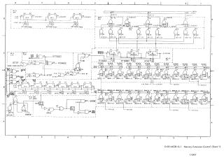
This document contains a comprehensive set of schematic diagrams and logic gate configurations for the Memory Extension Control system of a computer.
Key technical components and functions illustrated throughout the 43 pages include:
- Memory Control and Expansion: Detailed logic for memory extension control, including inhibit drivers, X and Y axis selection, and memory control logic (MM8I-A-1, MM8I-A-2).
- Memory Parity: Schematics for memory parity options, including parity error detection circuits (MP8I-0-1).
- Display and Plotter Control: Logic for display control (VC8I-0-1) and plotter control (VP8I-0-1).
- Real-Time Clock: Configuration and control logic for real-time clock options, including variable and crystal clock controls (KW8I-0-1 through 0-3).
- System Logic: Flow diagrams illustrating various states (Fetch, Defer, Execute, Break), timing manual functions, register output/input control, shift and carry gate controls, and major register gating.
- Hardware Specifications: Detailed circuit diagrams for components such as the 10-bit D-A converter (A607-0-1), major registers (M220-0-1), and teletype receiver/transmitter controls.
The document includes extensive logic gate layouts, wiring information, and technical notes regarding component replacement, signal states, and system-specific configurations for models such as the MC8I-A and MC8I-B.
Site structure and layout ©2025 Majenko Technologies