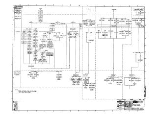
Processor Flow Chart
Order Number: XX-XXXXX-XX
This document consists of technical schematics and timing diagrams for the Digital Equipment Corporation PDP-8/E computer system. It includes the following components:
- Processor Flow Chart: A high-level logic diagram outlining the operational cycles (Fetch, Defer, Execute) and data pathways of the processor.
- Timing Diagrams: Detailed pulse-timing charts for Fast and Slow cycle operations, illustrating clock signals, memory control strobe signals, and internal memory interface timing.
- Major Registers and Logic Schematics: Several pages of detailed gate-level circuit diagrams for the system's "Major Registers" (M830/M831 modules), documenting component layouts, pin-outs, and logic connections.
- Bus Loads: A schematic detailing the bus load interface circuits, including diode matrices and signal termination for various control lines.
- Timing Generator: Schematics for the M830 timing generator module, showing the clock distribution and control signal generation logic.
The document provides the necessary engineering reference for the hardware implementation, register-level operation, and signal timing of the PDP-8/E processor architecture.
Site structure and layout ©2025 Majenko Technologies