Variable Clock R450
Order Number: I3-09150-04
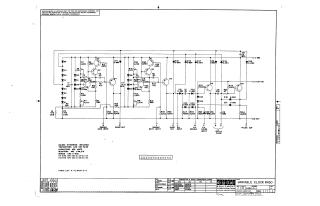
This document is a technical schematic for a "Variable Clock R450" circuit designed by Digital Equipment Corporation (dated 1988). The circuit diagram illustrates a complex transistor-based logic configuration featuring various input/output points, including Gate, Clock, Pulse, and Enable inputs. The schematic details the specific integration of resistors, capacitors, and diodes (specifically DEC 3639 transistors and D-664/D-662 diodes) required to manage clock signal distribution and conversion. It also provides reference notes regarding component specifications and links to a separate parts list (A-PL-R450-0-0).
Site structure and layout ©2025 Majenko Technologies