Pdp8 Memory Management Board
Order Number: M8416-0-1
This document contains the engineering schematics and technical board layout for the PDP-8 Memory Management board (M8416). It includes:
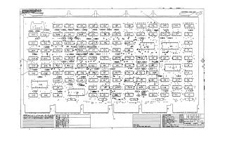
- Component Layout: A visual mapping of the board showing the placement of various electronic components (integrated circuits, capacitors, resistors, etc.).
- PCB Trace Diagrams: Detailed wiring patterns for both Side 1 and Side 2 of the circuit board.
- Logic Schematics: A comprehensive set of technical diagrams illustrating the logic circuits, including address relocation, memory field buffers, instruction field registers, bank select multiplexers, and break maps.
- Spare Components: A final page identifying unused logic gates and components available on the board design.
The document provides the necessary technical information to understand, manufacture, and troubleshoot the memory management functionality for the PDP-8 computer system.
Site structure and layout ©2025 Majenko Technologies