Option Board #2
Order Number: V400
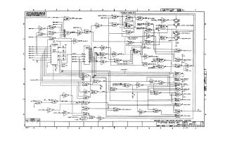
This document contains a series of technical schematic diagrams for the Digital Equipment Corporation (DEC) Option Board #2 (M8317-YB-1). The schematics detail the electronic logic circuits and connections required for several system functions, including:
- Memory Extension and Time Share Register Control: Logic for handling memory segments and time-sharing operations.
- Instruction and Data Fields: Circuitry for managing instruction and data field registers, including buffers for instruction saving and retrieval.
- Bootstrap and Autorestart Control: Logic circuits responsible for system startup, power-ok monitoring, and automatic restart sequences.
- ROM and Flag Logic: Schematics for ROM-based startup code, system status flags (including "Battery Empty"), and AC power monitoring.
- Bus Buffering: Detailed mapping of the bus buffer circuits (using 8837 buffers) that interface the system data lines with the board's internal logic.
These diagrams utilize standard TTL logic gate representations (e.g., 7400 series chips), flip-flops, and multiplexers to define the signal paths and hardware integration for the computer system.
Site structure and layout ©2025 Majenko Technologies