Data Break Interface
Order Number: M8362-0-1
Summary
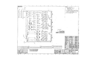
This document provides the technical schematics and circuit board layout for the "Data Break Interface" module. The document consists of three pages:
- Page 1: Details the physical component layout of the printed circuit board, including the placement of various integrated circuits (ICs), resistors, and capacitors. It also includes a parts list identifying specific DEC components (such as DEC 6314, 6384, and 6380) and notes on manufacturing standards, such as priority jumper configurations and voltage requirements.
- Page 2: Displays the logic circuit diagram for the interface, illustrating signal flow, buffer gates, and the integration of the MD (Memory Data) line. It identifies connections for signals like "Break Data," "Add Load Data," and various control lines.
- Page 3: Continues the logic schematic, focusing on the interface’s data handling and bus logic. It features notations regarding signal states (e.g., "H = Databus to MB," "L = Take Data Bus Plus MD to MB") and depicts the gating logic required to manage memory access and cycle control.
Site structure and layout ©2025 Majenko Technologies