Read Buffer
Order Number: M765
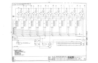
This document is a technical schematic for a Read Buffer module (model M765-0), designed by Digital Equipment Corporation in 1969. The circuit consists of a series of integrated circuits (primarily DEC7474N flip-flops and DM8570 shift registers) arranged to process data, likely for memory or input/output operations in a computer system. The schematic details the logic flow, including "Shift Enable," "Clock," and "Clear" control lines, as well as timing circuitry used for delay and windowing functions. It also provides specifications for components, including resistor values, capacitor types, and integrated circuit pin configurations.
Site structure and layout ©2025 Majenko Technologies