Negative Bus Converter
Order Number: M531
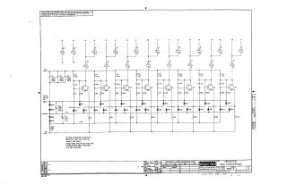
This document is a technical schematic for a Negative Bus Converter circuit designed by the Digital Equipment Corporation in 1970. The diagram details the electronic configuration, including the arrangement of eight identical channels consisting of integrated circuits (DEC7404), transistors (DEC3009B), diodes (D664), and various resistors and capacitors. It provides the wiring logic for input/output signals across an array of pins (BI through VI) and specifies voltage requirements, including +5V, -1.5V, -3V, and -15V supply rails.
Site structure and layout ©2025 Majenko Technologies