Negative Input Converter M506
Order Number: M506
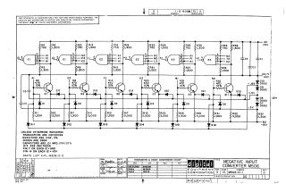
This document is an electrical schematic for a "Negative Input Converter" (Model M506) manufactured by Digital Equipment Corporation in 1967.
The circuit is designed to process input signals through a series of integrated circuits (DEC7420N NAND gates) paired with transistors (DEC3009B) and diodes (D664). Key features of the schematic include:
- Circuit Architecture: The layout consists of several parallel channels that utilize logic gates and transistor stages for signal conversion, supported by a network of resistors, capacitors, and diodes.
- Power Requirements: The board operates using a +5V supply line, with additional reference voltages at -1.5V and -3V, and a -15V supply line for the diode network.
- Component Specifications: The document provides a "Unless Otherwise Indicated" section specifying component values (1/4W 5% resistors, 0.01μF capacitors, etc.) and a transistor/diode conversion chart for maintenance and cross-referencing purposes.
- Regulatory/Legal: It includes a notice stating the schematic is proprietary and intended for test and maintenance purposes only.
Site structure and layout ©2025 Majenko Technologies