Parity Checkers and Gates
Order Number: M130
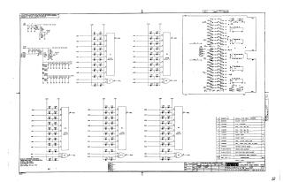
This document is a technical schematic for a Parity Checker and Gate circuit (Model MI30). The diagram outlines the wiring and component layout for multiple logic gates (using DEC 4008P integrated circuits) designed to process various data inputs (AA1-AL2, AN1-BV2) to provide even parity outputs. The document includes a detailed parts list specifying required resistors, diodes, capacitors, and the etched circuit board, alongside a diode/transistor conversion chart and general electrical specifications for the components.
Site structure and layout ©2025 Majenko Technologies