Fault Protection Board G838
Order Number: G838
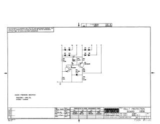
This document is a 1970 technical schematic from the Digital Equipment Corporation (DEC) detailing the circuit design for the "Fault Protection Board G838." The schematic includes a bridge-like configuration of diodes (D1-D9) connected to a transistor-based circuit featuring two transistors (Q1 DEC2219 and Q2 DEC2904), a 5.1V Zener diode (D5), and various resistors and a capacitor. The document also includes a transistor and diode conversion chart, providing industry-standard (EIA) equivalents for the proprietary DEC components used on the board.
Site structure and layout ©2025 Majenko Technologies