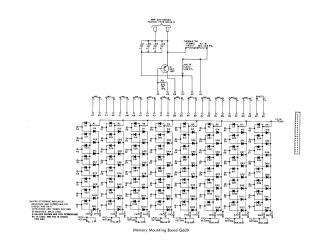
Memory Mounting Board G609
Order Number: XX-XXXXX-XX
This document is a technical schematic for a Memory Mounting Board (G609). It details the electronic circuitry layout, including:
- Component Array: A large matrix of diodes (D1 through D128) organized into rows and columns, typically used for memory addressing or signal routing.
- Support Circuitry: A configuration at the top of the diagram includes a transistor (Q1, DEC 1557), a thermistor (Fenwal), capacitors (C1–C4), and several resistors (R9, R10, R11) used for regulation or signal conditioning.
- Connectivity: The board features multiple "Read" and "Write" signal paths, various return lines (CDO, CHO, CLO, CPO, CTO, DDO, DHO, DLO), and extensive terminal points (labeled AF through BU).
- Specifications: The diagram provides specific component values, noting that unless otherwise indicated, resistors are 4,700 ohms (1/4W, 5%), diodes are D671, and capacitors are 50MFD 50V GMV. It also identifies specialized values for Ferrox-cube components (R11 at 100 ohms and R10 at 2700 ohms for EMI).
Site structure and layout ©2025 Majenko Technologies