RX50 Seek/Interface PCB
Order Number: XX-7A37B-9C
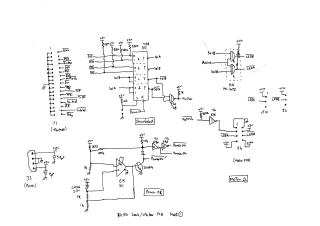
This document comprises a series of circuit diagrams detailing the electronic design of an RX50 disk drive, organized across different Printed Circuit Boards (PCBs) and functional blocks.
Seek/Interface PCB (Pages 1-4): This section outlines the core control and interface logic. It includes power supply management (J3, E15), drive and side selection (E12), and the processing of various sensor inputs from the disk drive's mechanical components (J2, J8). These sensors detect conditions like write protection, disk presence, and index pulses, generating critical control signals such as
Wr Prot,Rdy,Active, andIndex. Furthermore, it details the stepper motor driver circuitry (E2b, E2c) responsible for precise head positioning (J7) based onStepandDirsignals, and the initial stages of read/write control logic (E6a, E7a, E7b, E6b) which managesWrite Data (WD),Write Enable, and raw read/write signals for interaction with the Read/Write PCB (J9).Spindle Motor Speed Control PCB (Page 5): This page is dedicated to the circuitry that controls the rotational speed of the disk drive's spindle motor (J11). It features operational amplifiers (E2a, E1d, E26) in a feedback loop, likely involving a 555 timer (E1) for tachometer pulse generation (
Tacho Pulse). The design incorporates current tripping and integration circuits to ensure stable motor speed, along with connections for front panel LEDs (J4, J16) to indicate drive status.Read/Write (R/W) PCB (Pages 6-8): This section focuses on the data path for storing and retrieving information from the magnetic media.
- Page 6 illustrates the write circuitry, employing transistor drivers (2N4403, TPQ2907) to generate the precise current pulses and differential signals (
W-A,W-B) required for writing data onto the disk, based on inputs likeWrD,WrEn, andDly Wr En. - Page 7 describes the head switching logic, which utilizes an analog multiplexer (E4) to select and activate the appropriate read/write head (J14) for read, write, or erase operations, controlled by signals such as
WrEnandSELA. - Page 8 presents the read channel, responsible for amplifying the weak analog signals (
RdA,RdAB) received from the read heads using an amplifier (E1 MC3740). It includes an extensive RC/LC filter network for signal conditioning and converts the amplified, filtered analog signal into a digital data stream (Date Out,RdD) via internal one-shot and comparator stages, with a 78L05 regulator providing a stable 5V supply for the analog section.
- Page 6 illustrates the write circuitry, employing transistor drivers (2N4403, TPQ2907) to generate the precise current pulses and differential signals (
Overall, the document provides a comprehensive overview of the electronic components and their interconnections that enable the RX50 floppy disk drive's functionality, from basic power and motor control to sophisticated data handling.
Site structure and layout ©2025 Majenko Technologies