Rainbow Memory Extension
Order Number: XX-9A940-C0
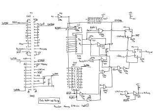
This document details the circuit diagrams for a "Rainbow Memory Extension," an add-on memory unit likely designed for a specific computer system (implied by "Rainbow"). It is presented across four sheets, each focusing on a different functional aspect of the memory extension:
- Data Buffer and Parity: This sheet illustrates the buffering of system addresses (SysAddr) and data (SysData), along with the generation and checking of memory parity. It includes logic for essential memory control signals like RAS (Row Address Strobe), CAS (Column Address Strobe), Read, and Write.
- RAM Control Buffers: This section focuses on generating and buffering the control signals required for multiple RAM banks. An 82S129 Programmable Logic Device (PAL) decodes system addresses and bank type to enable specific memory banks. Subsequent buffer stages prepare the Row Address Strobe (RAS), Column Address Strobe (CAS), and Write Enable (Wr) signals for up to three distinct RAM banks (RAS1/2/3, CAS1/2/3, Wr1/2/3). A bank selection switch array is also included for configuration.
- DRAM Address Multiplexing and Refresh: This sheet details the logic for multiplexing addresses for the Dynamic RAMs (DRAMs). It uses multiplexers to select between the system address (SysAddr) and a refresh address (RfshAddr), which is generated by a dedicated refresh counter, to form the final DRAM address. This mechanism is crucial for refreshing dynamic memory. Bank address decoding logic is also shown to enable specific memory banks based on the Bank Type.
- DRAM Arrays and Data Buffers: The final sheet illustrates the actual memory arrays, which comprise three banks of 4164 or 41256 DRAM chips. Each bank is configured with 8 chips, suggesting an 8-bit data width. Each bank receives its specific DRAM address and control signals (RAS, CAS, Wr) from the previous stages. A comprehensive set of bidirectional data buffers ("Din Dout") are included for interfacing the DRAM chips with the rest of the system, managing data transfer for each memory bank.
In summary, the document provides a comprehensive design overview for a memory extension, covering address management (buffering, multiplexing, refresh), control signal generation, parity handling, and the physical implementation of DRAM arrays with their data interfaces.
Site structure and layout ©2025 Majenko Technologies