PDP.9
Order Number: XX-3DAA0-90
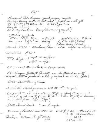
The PDP.9 is a general-purpose, parallel, binary computer featuring an 18-bit word length and a single-address architecture. It incorporates 8K (8192) 18-bit words of core memory with a 2μs cycle time.
Key Components and Architecture:
- Registers: The system includes an 18-bit Accumulator (AC), Memory Buffer (MB), a 13-bit Program Counter (PC) to track instruction flow, and a Memory Address (MA) register. An Instruction Register (IR) holds the first 5 bits of a 17-bit instruction. A 1-bit Link (L) extends AC capabilities for arithmetic operations, which support both two's complement and one's complement. An Arithmetic Register (AR) is used for key operations.
- Memory System: The main memory uses a 2.5D organization (MC-70B type) with a 1μs read-modify-write cycle. A 3D read operation process involves word, digit, sense lines, and a sense amplifier. A separate Control Memory, comprising 64 addressable 36-bit locations (30 bits for common data, 6 for the next address), guides operations.
- Peripherals: Standard peripherals include a Paper Tape Reader (PTR) at 300 lines/sec and a Punch (PC03) at 50 lines/sec, both handling alpha and binary data. A TTY Keyboard allows 10 characters/sec I/O.
- I/O and Data Transfer: The system features a Real-Time Clock (RTC) with a 60 cps counter and a Program Interrupt (PI) facility activated when peripherals are ready. Direct Memory Access (DMA) enables high-speed data transfers, with a Data Channel (DCH) supporting medium-speed peripherals through 3-4 cycle break operations, managing dedicated word count and address locations.
Instruction Set and Operations: The instruction set covers various operations for data manipulation (e.g., AND, XOR), memory access (LAC, DAC, DZM), program flow control (JMP, JMS for subroutines, ISZ for increment and skip if zero, SAD for skip if AC content differs), and I/O control (IORS to read flags, CAF to clear flags, ION/IOF for interrupt management, KSF for keyboard skip, KRB to read keyboard buffer). Auto-indexing is supported for indirect memory addresses (locations 10-17). The document provides detailed examples for logical operations, arithmetic computations, and subroutine calls.
Hardware Logic and Control: The document also delves into the underlying hardware logic, describing various gates (Diode Gates for AND/OR, Nand, Nor), pulse amplifiers, and delay networks. It details different types of Flip-Flops (e.g., JK Flip-Flop) and their roles in signal processing and state control, including specific timing characteristics and interconnections. The power control system and its interaction with internal clocks and registers are also outlined.
Site structure and layout ©2025 Majenko Technologies