Core Fundamentals
Order Number: XX-0F4FE-52
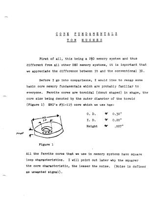
This document, "Core Fundamentals," by Tom Hughes, provides an in-depth explanation of core memory systems, specifically focusing on a 2D memory architecture. It contrasts this with conventional 3D systems and begins by detailing the basic characteristics of ferrite cores: their toroidal shape, physical dimensions (e.g., 0.30" outer diameter, 0.20" inner diameter, 0.007" height for the EMI's #31-115 core), and their crucial "square loop" (B/H loop) magnetic properties that minimize noise.
The text explains how magnetic states ('0' or '1') are written and read by applying currents. It differentiates between reversible flux changes (from half-select currents) and nonreversible flux changes (from partial or full-select currents), describing the resulting voltage outputs on the sense winding. Two important timing parameters, "Peaking Time" and "Switching Time," are defined. The write and read cycles are outlined, noting that a read cycle produces a signal of opposite polarity. The document also addresses how temperature variations affect the B/H loop, necessitating current amplitude adjustments.
Moving to core organization, it explains the "coincident current technique" used in stacked arrays, illustrating a 4K memory as a 64x64 matrix. A core is selected by applying half-currents to intersecting horizontal (X) and vertical (Y) drive lines. The "inhibit" wire is introduced as a method to write a '0' by opposing a half-current. A significant portion is dedicated to noise management: half-disturbed cores generate small outputs, requiring sense windings to be threaded in specific patterns (e.g., half the cores in one direction, half in the opposite) to cancel cumulative noise.
The concept of a "Worst Case Pattern (WCP)" highlights "delta noise," which arises from the imperfect cancellation of half-disturbed 'one' and 'zero' signals, complicating signal discrimination. To mitigate large noise spikes caused by current transients, especially from the inhibit line in 2D systems, "staggering" is used—delaying the word line turn-on relative to the digit line to allow transients to decay.
In the 2D memory architecture, the X dimension is dedicated to word addressing, while the Y (digit or bit) dimension performs a dual function for both address and data (acting as an augment or inhibit line). The memory stack is a planar array, with a 16x512 arrangement designed for balanced electrical length. "Word current phasing" allows word lines to drive two addresses based on current direction, enabling 256 lines to access 512 addresses. The 256 drive lines are decoded using a 16x16 matrix, with MA BIT 5 controlling the phasing (selecting between upper or lower 4K memory segments). Finally, the memory cycle is characterized as "read pause write," where a fixed pause (e.g., 300 ns) is implemented between read and write operations to accommodate data processing and cable delays, due to the absence of a memory buffer.
Site structure and layout ©2025 Majenko Technologies