RX02 Emulator Interface
Order Number: XX-D3EE4-7F
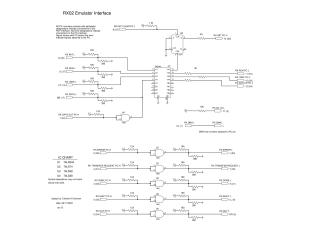
This document presents the circuit diagram for an RX02 Emulator Interface, designed to bridge communication between a PDP interface and a PC interface. The design incorporates several integrated circuits (ICs) for buffering, logic, and control.
Key components include:
- U1 (74LS244 Octal Buffer): Used to transmit signals from the PDP interface (e.g., RX INIT L, RX RUN L, RX 12BIT L, RX DATA L) to the PC interface (e.g., RX RUN PC L, RX 12BIT PC L, RX DATA IN PC L).
- U2 (74LS74 D-type Flip-Flop): Manages initialization, controlled by "RX INIT CLEAR PC L" to generate "RX INIT PC H".
- U3 and U4 (74LS38 Quad 2-Input NAND Gates): Primarily function as inverting buffers, processing control signals from the PC (e.g., RX ERROR PC H, RX TRANSFER REQUEST PC H, RX DONE PC H, RX SHIFT PC H, RX OUT PC H) and converting them into active-low signals for the PDP interface (e.g., RX ERROR L, RX TRANSFER REQUEST L, RX DONE L, RX SHIFT L, RX OUT L). U4 also buffers "RX DATA OUT PC H".
The diagram notes that alphabetic designations correspond to PDP interface connections, while numeric designations relate to PC interface connections. Signal names prefixed with "PC" indicate attachment to the PC. The "RX DMA L" signal is noted as not having an assigned PC pin. The circuit includes various resistors for pull-ups and voltage division.
The document was designed by Charles H Dickman on June 11, 2003, with revision B.
Site structure and layout ©2025 Majenko Technologies