M767
Order Number: XX-A6CFD-17
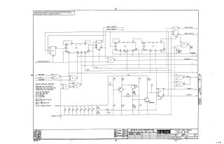
This document is a proprietary schematic diagram for a "Clock and Skew Delay M767" circuit, copyrighted by Digital Equipment Corporation in 1970 and intended solely for test and maintenance purposes.
The circuit's primary functions are:
- Clock Generation: An oscillator built around a crystal (CRI) and transistors (Q1, Q2, Q3) generates fundamental clock signals.
- Clock Processing and Output: Logic gates (DEC7400, DEC7402) and JK flip-flops (DEC7473, specifically E7) process these signals to produce various clock outputs, including "CLOCK L," "CLOCK H," "WRITE CLOCK L," and "WRITE CLOCK H."
- Skew Delay Generation: A chain of 4-bit shift registers (DEC8281, E2, E4, E6) and JK flip-flops (DEC7473, E5) is utilized to create controlled delays and "skew" in signals. Inputs like "DELAY STROBE H/L" and "START SKEW DELAY H" likely control this delay mechanism, providing outputs such as "SKEW DELAY L" and other timing signals.
The circuit predominantly uses standard TTL (Transistor-Transistor Logic) integrated circuits for logic functions and discrete transistors for the oscillator, along with passive components like resistors and capacitors. Default component specifications are provided, such as 10K, 1/4W, 5% resistors and 0.01uF, 100V, 20% capacitors.
Site structure and layout ©2025 Majenko Technologies