M752
Order Number: XX-F5135-4C
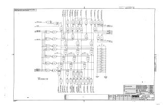
This document is a proprietary schematic diagram from Digital Equipment Corporation, dated November 4, 1968, for an "INSTRUCTION DECODER M752". Its stated purpose is for "TEST AND MAINTENANCE" only.
The circuit is composed primarily of various types of DEC74xxN series integrated circuits, specifically NAND and NOR gates and buffers, along with resistors and capacitors. It is designed to operate with standard TTL logic levels, requiring +5V and GND for its ICs.
Key inputs include signals prefixed with "TT" (e.g., TTCLI, T1/T2 SKIP, TTLL, TT OFF/ON, TTINCR, TTRL, TT ON), which likely relate to timing or specific system operations. It also takes "BMB" signals (e.g., BMB 6(0) through BMB 8(1), BMB 9(1), BMB11(1)), which are probably bus-related data bits. Initialization signals ("INITIALIZE -ABI", "INITIALIZE ACI") are also present.
The primary function of the circuit, as indicated by its title and main outputs, is to decode instruction words. It provides two main output buses: "I-LINE OUT O-63" and "I-LINE OUT 64-127," suggesting it decodes a large instruction word, potentially up to 128 bits, into two 64-bit segments.
Site structure and layout ©2025 Majenko Technologies