M706
Order Number: XX-D9083-5F
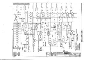
This document is a detailed schematic diagram for the Digital Equipment Corporation (DEC) Teletype Receiver M706.
Its primary purpose is to receive serial data, likely from a teletype communication line, and convert it into an 8-bit parallel output format.
The circuit features:
- Input Stage: Signal conditioning and buffering for the serial input, including 'RECEIVED' data and 'BAUD' clock signals.
- Core Logic: A network of integrated logic gates (NAND, NOR, AND, XOR) and D-type flip-flops (labeled E5 through E10 for 'BIT 1' through 'BIT 8'). These components form a multi-stage shift register, responsible for sequentially capturing and storing the incoming serial bits to produce the parallel output.
- Control and Timing: Various control and status signals such as 'BUFFER STROBE,' 'SKIP STROBE,' 'P.I. REQ.' (Programmed Interrupt Request), 'READER RUN,' 'SHIFT,' 'I/O CLEAR,' 'FLAG,' 'STOP TIME,' and 'PRESAMPLING' to manage the data reception and processing.
- Outputs: Provides parallel 8-bit data outputs (BIT 1 OUTPUT through BIT 8 OUTPUT) along with the 'CLOCK @ BAUD' and other interface signals.
- Component Details: Specifies component types, power supply requirements (+5V, +3V), and includes a transistor and diode conversion chart.
The schematic is intended for test and maintenance purposes and is proprietary to Digital Equipment Corporation.
Site structure and layout ©2025 Majenko Technologies