M514
Order Number: XX-CDDB6-71
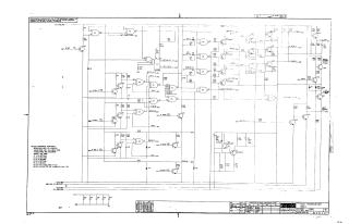
This document is a schematic diagram for the Digital Equipment Corporation (DEC) M514 Bus Transceiver, copyrighted 1970.
Key features and information provided:
- Purpose: Furnished specifically for test and maintenance purposes, containing proprietary circuit information.
- Components: The circuit design incorporates various integrated circuits (ICs) from the DEC74xx series (DEC7440, DEC7400, DEC7486), along with DEC9601 and DEC384 chips. It also utilizes discrete components, including DEC30998 and DEC2904 transistors, D003 diodes, resistors, and capacitors.
- Power Supplies: The system operates using multiple voltage rails: +5V, -2.4V, -3.3V, and -15V.
Functionality (inferred from signal names): The schematic details logic for controlling bus operations, including:
- Function Setting/Clearing: Signals like "SET FUNCTION L-ADI" and "CLEAR FUNCTION L-AM2."
- Bus Selection: Inputs such as "BE2 B SEL 0," "BM2 B SEL 1," and "BK1 B SEL 2."
- Data Matching/Status: Signals like "MATCH 4 H-ALI," "MATCH 2 H-ARI," "MATCH 1 H-ANI," and "REWIND D7 STATUS L."
- Read/Write Control: Signals such as "WRITE STROBE H-BT2," "RFWD H-BJI" (Read Forward), "R REW H-BFI" (Read Rewind), and "R WRE H-BNI" (Read Write).
- Strobe and Pulse Generation: "B SET PULSE H-B12" and "LRCC STROBE H."
- Remote/Local Selection: "SELECT REMOTE L-AF1."
Technical Notes: Provides standard specifications for resistors (2.7K, 1/4W, 5%) and capacitors (0.1uF, 100V, 20%) unless otherwise indicated. It also includes pin assignments for IC power, and a conversion chart for DEC transistor and diode part numbers to their EIA equivalents.
Site structure and layout ©2025 Majenko Technologies