M506
Order Number: XX-4599F-39
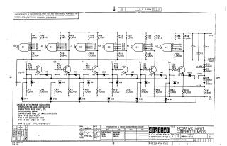
This document is an electronic schematic for the Digital Equipment Corporation (DEC) M506 Negative Input Converter, copyrighted in 1967. It is provided for test and maintenance purposes and contains proprietary circuit information.
The circuit design utilizes several integrated circuits (DEC7420N, configured with Pin 7 to GND and Pin 14 to +5V), which process multiple input signals. These signals are then fed into multiple transistor-based output stages (using DEC3009B transistors) that include diodes (D664) and various resistors. The circuit operates with primary power supplies of +5V and -15V, and also generates intermediate negative reference voltages (-0.6V, -1.5V, -3V) using D662 diodes.
Component specifications are detailed, indicating resistors are 1/4W, 5%; diodes are D664 (except D662 for voltage references); and capacitors are .01 MFD, 100V, 20%. The document also includes a Transistor & Diode Conversion Chart (DEC to EIA equivalents) and references a separate parts list (A-PL-M506-0-0). A revision history is also present.
Site structure and layout ©2025 Majenko Technologies