M401
Order Number: XX-3B095-76
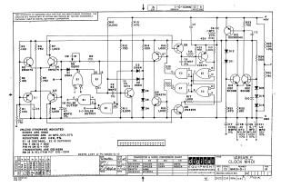
This document is a schematic diagram for a circuit titled "VARIABLE CLOCK M401," designated as M401-0-1. It was copyrighted in 1967 by Digital Equipment Corporation (DEC) and is intended solely for test and maintenance purposes, containing proprietary circuit information.
The schematic details a clock circuit utilizing various discrete components and integrated circuits, operating with a +5V power supply and Ground.
Key components and specifications include:
- Resistors: Generally 1/4W, 5%, with specific values indicated. R8 is a 10%-78PR Helitrim Potentiometer.
- Capacitors: Generally 0.1 MFD, 100V, 20%, with specific values and types (e.g., Mylar) indicated for others.
- Diodes: Primarily D662 (equivalent to 1N645) unless otherwise specified, with D664 (1N3606) and other diodes (D11-D15) also present.
- Transistors: A mix of types, including 2N4274, DEC3009B (equivalent to 2N3009), DEC6534D (equivalent to MPS6534), and general DEC4258 (equivalent to 2N4258) transistors.
- Integrated Circuits (ICs):
- E1 series: DEC7400 (standard TTL NAND gates).
- E2 series: DEC74H00 (high-speed TTL NAND gates).
- Standard TTL pinout: Pin 7 is Ground, Pin 14 is +5V.
The circuit features both (+) Pulse Output and (-) Pulse Output. The drawing was created on September 11, 1967, and includes a revision history table.
Site structure and layout ©2025 Majenko Technologies