M253
Order Number: XX-360D0-BD
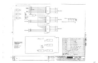
This document is a schematic diagram for a 12-bit, 16-word memory module, identified as M253-0-1, designed by Digital Equipment Corporation in 1971 (Revision B).
The circuit's core functionality relies on:
- Three DEC7489 Integrated Circuits (E1, E2, E3), which are 16-word by 4-bit RAMs, collectively forming the 12-bit wide memory.
- DEC1074H00 (7400 series NAND gates, E4) for implementing control logic, including "CHIP SELECT".
The memory module features:
- Address Inputs: Four address lines (K1, S1, A1, N1) to select one of the 16 words.
- Data Inputs: Twelve data lines (D0-D11) for writing data into memory.
- Data Outputs: Twelve data lines (O0-O11) for reading data from memory.
- Control Signals: "WRITE ENABLE" and "CHIP SELECT I".
Support circuitry includes various capacitors (e.g., 0.01uF for decoupling, a 68uF electrolytic for bulk filtering) and resistors (e.g., 330 ohm, 750 ohm) for power filtering and biasing. Power is supplied at +5V, with specific pin assignments for power and ground noted for the ICs.
A comprehensive parts list details all components used, including the specific ICs, resistors, capacitors, and mechanical items like a "FLIP CHIP" handle and eyelets, indicating the module is designed for an etched circuit board. The drawing was made by Nancy Hoore.
Site structure and layout ©2025 Majenko Technologies