M139
Order Number: XX-3D25E-5C
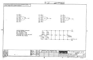
This document is a schematic diagram for a 3-8 Input NAND Gate circuit, specifically model M139-0-1, manufactured by Digital Equipment Corporation (DEC) and copyrighted in 1969.
Key information presented:
- Purpose: The schematic is for test and maintenance, and the circuits are proprietary.
- Logic Gates: It illustrates three separate 8-input NAND gates (labeled E1, E2, E3), each using 6 inputs in this configuration (e.g., B1-E2 for E1). The integrated circuits (ICs) used are DEC1074H30.
- IC Power: Each IC requires +5V on Pin 14 and Ground (GND) on Pin 7.
Component Specifications (unless otherwise indicated):
- Capacitors: 0.01 MFD, 100V, 20% tolerance. A specific electrolytic capacitor (C5) is 39 MFD, 10V, 10%.
- Resistors: 1/4W, 5% tolerance, with specific values of 330 Ohm (R1, R3) and 750 Ohm (R2, R4) shown in the filtering section.
Power Filtering: A section with resistors and capacitors provides filtering and potentially derives +3VUI and +3VVI signals from the +5V supply.
- Document History: The drawing was completed by R. Gutierrez on 3-4-69, checked by A. Yauga on 3-6-69, and engineered by D.E.O. on 4-7-69. The document is at Revision D.
Site structure and layout ©2025 Majenko Technologies