G913
Order Number: XX-A9511-8C
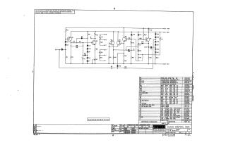
This document is a proprietary schematic diagram for the "CLOCK CONTROL G913" circuit, copyrighted by Digital Equipment Corporation (DEC) in 1968.
Key features and information include:
- Purpose: The schematic is furnished solely for test and maintenance purposes.
- Circuit Diagram: A detailed electronic circuit is displayed, featuring numerous components such as transistors (Q1-Q6), diodes (D1-D24), resistors (R1-R22), and capacitors (C1-C9). It operates with +10V, Ground (GND), and -15V power rails, and shows various labeled input/output points.
- Parts List: A comprehensive "PARTS LIST" details each component by its reference designation, provides a description (e.g., resistance/capacitance values, tolerances, wattage for resistors, voltage ratings for capacitors, transistor types), and lists the corresponding DEC part numbers.
- Transistor & Diode Conversion Chart: This chart provides cross-references between DEC part numbers and their EIA equivalents for specific transistors and diodes used in the circuit.
- Document Details: It specifies the circuit as a "PRINTED CIRCUIT" with part number C CS 6913-0-1, and includes design and approval dates from May/June 1968.
Site structure and layout ©2025 Majenko Technologies