G221
Order Number: XX-449FD-D0
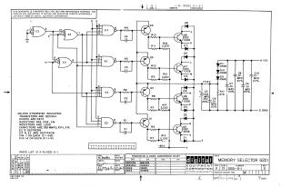
This document is a proprietary schematic diagram for a Memory Selector G221, designed by Digital Equipment Corporation, with the initial drawing dated January 3, 1967, and a revision level of D. It is intended solely for test and maintenance purposes.
The circuit features:
- Digital Logic Gates: Primarily uses DEC7400N (E2) and DEC7440N (E1, E3) integrated circuits, which are likely NAND gates, configured with standard TTL power (Pin 7 to GND, Pin 14 to +5V).
- Transistors: A series of transistors (Q1-Q8), including types like DEC2904 and DEC1008, many of which are part of driver or switching stages.
- Diodes: Numerous diodes (D1-D11), with types such as D662 and D672.
- Passive Components: Resistors (R1-R17) and capacitors (C1-C10) are used throughout the circuit for biasing, filtering, and coupling.
- Power Rails: Operates with multiple voltage rails, including +5V, +3.2V, -30V, and Ground (GND).
Component Specifications (unless otherwise indicated):
- Transistors: DEC2904
- Diodes: D672
- Resistors: 1/4W, 5% tolerance (some specific values of 1,500 ohms are noted, and several 2,200 ohm resistors are explicitly shown).
- Capacitors: 330 MMFD (pF), 100V, 5% tolerance (some specific values like 0.01 MFD and 6.8 MFD are noted).
A Transistor & Diode Conversion Chart is provided, listing DEC part numbers (e.g., DEC1008, DEC2904, D662, D672) and their corresponding EIA equivalents (e.g., MM1008, 2N2904, IN645, IN3653). The document also references a separate Parts List (A-PL-G221-0-1).
Site structure and layout ©2025 Majenko Technologies