50Ω OR BUS DRIVER B683
Order Number: B683-0-1
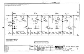
This document is an electrical schematic diagram for a 50Ω OR Bus Driver circuit, designated as B683. The circuit is designed with three distinct output stages (OUTPUT 1, OUTPUT 2, OUTPUT 3), each employing a pair of transistors (e.g., Q1/Q2 for Output 1). The design incorporates various transistors (2N4258, DEC 3009B, DEC 2904A), resistors, diodes (D662, IN752A 5.6V), and capacitors (.01 MFD, 6.8 MFD). Power is supplied at +10V and -15V, with several ground connections. Input/control points are labeled P, E, F, J, K, S, T. General specifications state that resistors are 1/4W, 5% and diodes are D664, unless otherwise indicated. A conversion chart for transistors and diodes (DEC to EIA part numbers) is provided. The schematic is proprietary to Digital Equipment Corporation, copyrighted 1967, and intended solely for test and maintenance purposes. The drawing was made by M. Waller on March 14, 1967, and the revision shown is 'C'.
Site structure and layout ©2025 Majenko Technologies