VARIABLE DELAY LINE B312
Order Number: B312-0-1
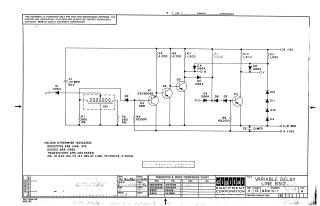
This document is an electronic schematic diagram for a Variable Delay Line, model B312, copyrighted by Digital Equipment Corporation in 1966. It provides a detailed circuit layout featuring various components including transistors (Q1-Q4), diodes (D1-D12), resistors (R1-R11), capacitors (C1, C2), and a specific delay line component (DEI, ESC No. 73-63 with 250ns delay and 500Ω impedance). The schematic indicates input (LO) and output (UO) points, along with connections to power rails (+10V, -15V, and ground).
Accompanying the diagram are notes specifying general component characteristics (e.g., resistors are 1/4W, 10%; diodes are D662; transistors are DEC3639B unless otherwise indicated). A "Transistor & Diode Conversion Chart" maps Digital Equipment Corporation (DEC) part numbers to equivalent EIA standard part numbers. The document explicitly states that the schematic is for test and maintenance purposes only, and the circuits are proprietary.
Site structure and layout ©2025 Majenko Technologies