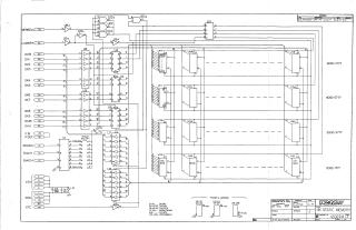
4k Static Memory
Order Number: F280
Summary: This document is a technical schematic for a 4K Static Memory board designed by PC/M (dated November 1, 1977). The circuit utilizes a 2102-family memory architecture, organized into four banks of memory corresponding to the address ranges 0000–1777, 2000–3777, 4000–5777, and 6000–7777. The diagram details the integration of data inputs (DX0–DX11), address lines (EMA0–EMA2), and control logic (MEMSEL, LXMARH, PIN/POUT) using a variety of 74-series logic gates (74L04, 74LS75, 74366, 74L00) to manage memory access and bank selection.
Site structure and layout ©2025 Majenko Technologies