Module Utilization
Order Number: XX-XXXXX-XX
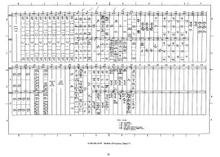
This document consists of two sheets of technical diagrams (sheets 1 and 2) titled "Module Utilization" for the D-MU-8L-0-18 system. The diagrams provide a comprehensive mapping of a computer system's backplane or logic board layout.
Key aspects of the document include:
- Grid Layout: The pages use an alphanumeric grid to pinpoint specific module positions (numbered 1 through 44).
- System Functions: The charts detail various control panel operations, memory functions (including parity, data break, and power fail), timing signals, and bus pathways.
- Component Detail: Each grid location defines the signal, logic, or component associated with specific board slots, including input/output drivers, registers, power regulators, and memory controllers.
- Options: The bottom of Sheet 1 notes specific configuration options, such as High-Speed Reader/Punch support and the requirement to use G852 if a memory parity option is installed.
- Control Logic: Sheet 2 focuses heavily on execution cycles (Fetch, Defer, Execute), strobe signals, and various system controls (Print, Teleprinter, Clock, and data bus management).
Site structure and layout ©2025 Majenko Technologies