Module Utilization
Order Number: XX-XXXXX-XX
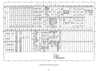
This document provides a comprehensive set of two-sheet diagrams detailing the "Module Utilization" for a computer system (specifically associated with the D-MU-8L-0-18 technical documentation).
The diagrams serve as a reference map for the hardware configuration and logic board layout, illustrating:
- Pin and Signal Mapping: The charts map specific signals and components across a grid of connectors (numbered 1 through 44) and usage categories.
- Component Roles: It identifies the placement and function of various system elements, including registers (REG), bus drivers, memory control, parity logic, data paths, and timing/control signals (e.g., fetch, execute, defer, and various strobe/interrupt signals).
- System Options: The document outlines specific hardware options, such as Data Break, Memory Parity, Power Fail, and High-Speed Reader/Punch, noting how certain modules are substituted (e.g., replacement by G052 if Memory Parity is installed).
- Control Panel Connections: It includes details regarding the Control Panel interface, input/output operations, and peripheral support (like printers and teleprinters).
Essentially, these sheets function as the technical blueprint for the physical and logical integration of the system's modules within the hardware chassis.
Site structure and layout ©2025 Majenko Technologies