Flip Chip Modules
Binary to Octal Decoder
Order Number: XX-XXXXX-XX
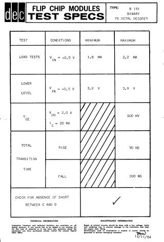
This document provides the technical specifications, test conditions, and a circuit schematic for the R151 Binary to Octal Decoder Flip Chip module.
Summary of Technical Specifications:
- Load Tests: 1.8 mA minimum to 2.2 mA maximum.
- Lower Level: 3.2 V minimum to 3.9 V maximum at -0.5 V input.
- $V_{CE}$: 300 mV maximum.
- Total Transition Time: 70 ns rise time and 300 ns fall time maximums.
- Maintenance Note: Includes a verification step to check for shorts between terminals C and D.
Maintenance Guidance: The document emphasizes that printed circuit repairs should be performed with a low-voltage, cool soldering iron to prevent copper lifting. Additionally, it advises that oscilloscopes used for troubleshooting must be grounded to prevent damage from transients. The second page contains a detailed circuit schematic identifying component values and transistor/diode types.
Site structure and layout ©2025 Majenko Technologies