16k 12-Bit Base Board
Order Number: C133
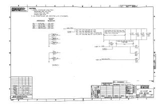
This document is a comprehensive technical schematic for a 16K, 12-bit Base Board. The document details the circuitry required for memory operations and data drive functions, specifically involving:
- Memory Addressing: Logic for bank selection (0-16K up to 48K-64K).
- Drive Logic: Includes detailed X-drive and Y-drive schematics for memory management.
- Sense Inhibit Circuits: Contains schematics for sense inhibit processing across 12 individual bits (Bit 0 through Bit 11), including the associated transistor logic, transformers, and signal timing controls for memory read/write cycles.
- Power and Support: Includes filtering, voltage regulation, and signal timing reference points (strobe timings and inhibit times) necessary for the operation of the memory board.
Site structure and layout ©2025 Majenko Technologies