Switch Filter
Order Number: W726
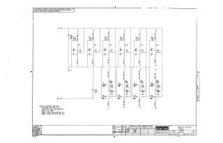
This document is a technical schematic for a W726 Switch Filter circuit board, produced by the Digital Equipment Corporation in 1970. The schematic illustrates the electrical layout for a series of six switch inputs (labeled V1, V2, U1, U2, T2, and S2) and four load outputs (R1, R2, N2, and P2). The circuit utilizes a network of resistors, capacitors, and diodes (specifically IN750 and IN746A types) to manage signal filtering. The document also includes general component specifications and a transistor/diode conversion chart for maintenance and testing purposes.
Site structure and layout ©2025 Majenko Technologies