Delay Line W300
Order Number: W300
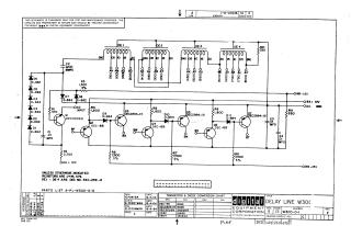
This document is a technical schematic for a Delay Line circuit (W300) designed by the Digital Equipment Corporation in 1964. The circuit utilizes four delay elements (DE1–DE4), a series of transistors (including DEC3009B and DEC2894-1B types), and multiple diodes to manage signal propagation. The diagram includes a transistor and diode conversion chart and indicates the required power inputs, specifically -15V (OAB/OBB) and +10V (OAA/OBA). It is intended for test and maintenance purposes and remains the proprietary property of the manufacturer.
Site structure and layout ©2025 Majenko Technologies