Rs-d-r211 Ma, Mb, Pc
Order Number: R211
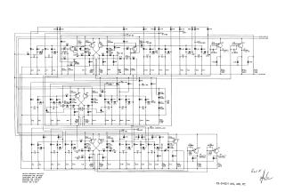
Summary This document is a technical schematic diagram for a digital circuit component, specifically labeled as the "MA, MB, PC" unit. The circuit features an extensive array of transistors (DEC3639), diodes (D-664), resistors, and capacitors. The schematic illustrates the signal flow and interconnection logic for various control and data functions, including inputs/outputs for "Count MB," "PC to MB," "Data to MB," "Data Address to MA," and "CM MB to MA." The design utilizes multiple buffered outputs and control signals operating between a +10V and -15V power rail, likely representing a portion of a larger vintage computing system's central processing or memory management logic.
Site structure and layout ©2025 Majenko Technologies